
PCB vias: technologies, fabrication, and design rules
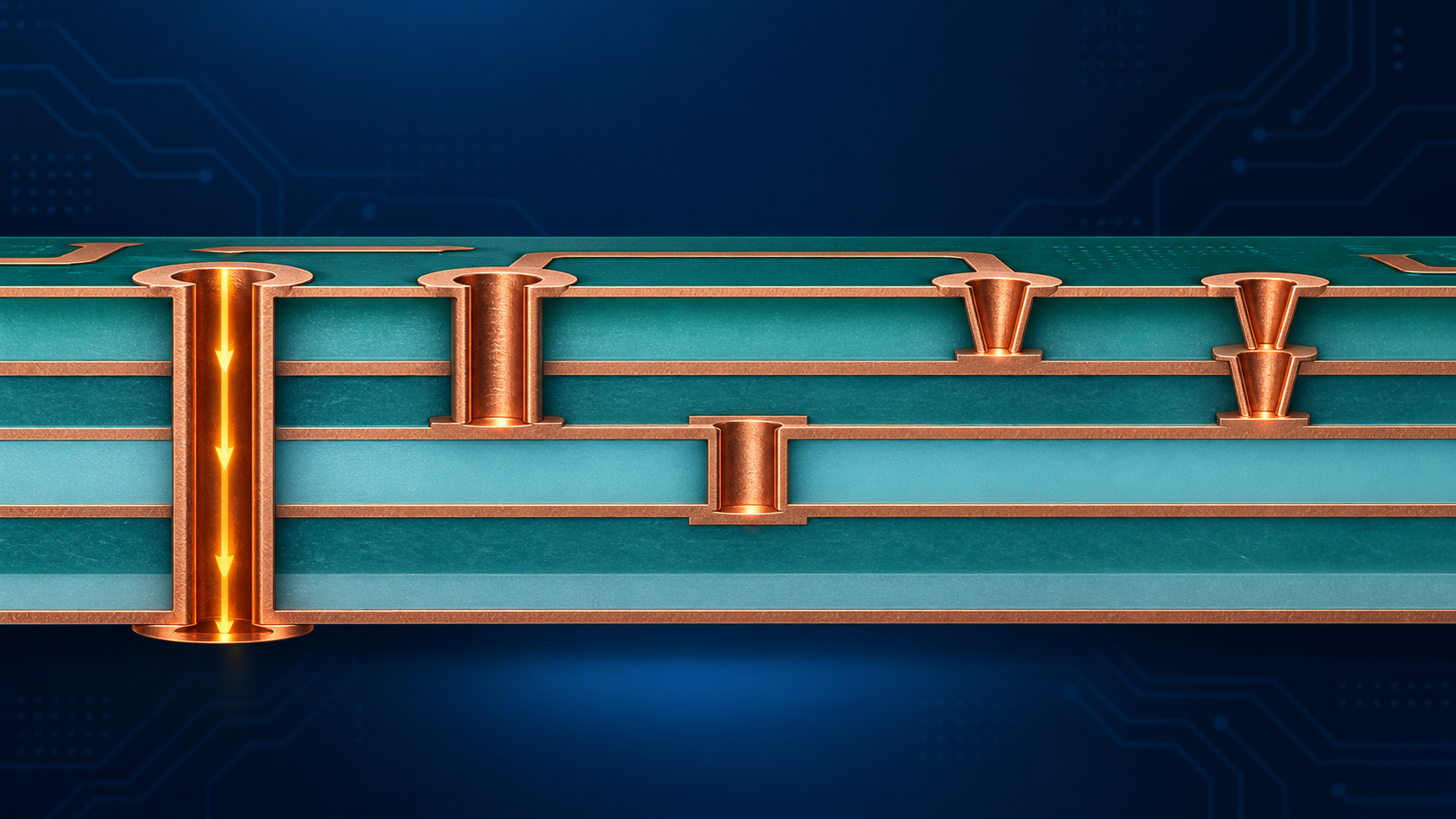
Choose through, blind, buried, or microvias for the stack-up, density, current, reliability, and frequency; master pads, annular rings, antipads, filling, stubs, and HDI transitions.
Written and technically reviewed byElectroDesignForge Engineering Team
View the editorial process📖 Definition
A via is a conductive interconnection between layers of a printed circuit board. It combines electrical geometry — pads, annular ring, hole, barrel copper, and plane clearances — with a specific fabrication sequence. A via is therefore not a universal dimension: a structure that is easy for one fabricator can be unavailable or unreliable for another.
A via can change a signal layer, join a power plane, remove heat, provide a return path at a layer transition, or escape a dense BGA. Selecting it means balancing the available stack-up, cost, routing density, DC current, thermal-cycle reliability, and high-frequency behaviour.
Use the PCB Via Calculator to estimate resistance, voltage drop, loss, temperature rise, capacitance, inductance, and reactance for a via path. It is a pre-sizing aid: the fabricator’s design rules and qualification requirements remain the manufacturing authority.
Via families at a glance
| Technology | Connected layers | Typical process | Main benefit | Main trade-off |
|---|---|---|---|---|
| Through via, or PTH | One face to the other; may connect all layers | Mechanical drill after lamination, then plating | Economical, robust, good for through-hole parts and planes | Uses space on every layer; creates a stub when the signal does not use the full board depth |
| Blind via | An outer layer to one or more inner layers | Controlled drilling before/after a lamination step, depending on the stack-up | Frees distant layers; can reduce a stub | More process steps and registration constraints |
| Buried via | Internal layers only | Drill and plate an inner core, then laminate | Consumes no outer-layer area | More complex cost, lead time, and stack-up |
| Laser microvia | In practice, usually adjacent layers | Laser ablation followed by plating | Very small diameter; BGA escape and HDI | HDI capability, material, aspect ratio, and reliability must be confirmed |
| Stacked microvias | Several HDI transitions on one axis | Sequential lamination; filling/capping is often required | Extremely compact vertical connection | Demanding process; interfaces and thermal cycles are critical |
| Staggered microvias | Several HDI transitions offset from one another | Sequential lamination | Avoids stacking every interface on one axis | More routing area and intermediate pads |
IPC-6012F covers rigid PCB constructions that include plated through-holes, blind/buried vias, and microvias. That does not make any standard value an automatic production capability: always obtain the offered DFM guide and stack-up.
Through vias: the default choice, with limits
A PTH (plated through-hole) is mechanically drilled through an already laminated board. Its hole wall is activated and plated; the deposited copper makes the barrel that connects the outer pads and any intended internal layers.
It is well suited to non-critical signals, power distribution, thermal vias, and moderately dense boards. A PTH connects an inner layer only where a pad is defined. On planes it must not connect to, copper is removed around the hole: this is the antipad or clearance.
The PTH stub
If a signal changes from L1 to L3 on an eight-layer board, a through via still has a barrel section from L3 down to the opposite face. That unused portion is a stub. At low frequency it is often harmless. As edge rates increase, it becomes a resonant shunt that can degrade the eye diagram.
Choose one of the following with the fabricator and after checking the interface:
- Accept the stub when the signal budget allows it.
- Change layer assignment or topology to shorten the unused length.
- Use a blind via or an HDI structure.
- Specify backdrilling: a controlled drill removes part of the unused barrel while leaving a margin near the connection layer.
Backdrilling is a fabrication operation that must be stated explicitly: diameter, depth, tolerance, layers to preserve, and mechanical keep-outs. It should never be introduced as a late geometric correction.
Blind and buried vias: density without treating the process as ordinary
A blind via starts on an outer face and ends on an internal layer. A buried via is entirely internal: it is made on a subset of layers before the remaining layers are laminated around it.
These structures remove pads and clearances from layers that do not take part in the connection. They are useful beneath a BGA, beside a dense connector, or where internal routing layers are already full.
They require an early fabrication discussion:
- which layer pairs are permitted for each via type;
- at which step drilling happens and how many lamination cycles are needed;
- which drill targets and registration tolerances are guaranteed;
- whether the fabricator mandates internal target-pad sizes;
- whether plating, cleaning, and inspection match the required reliability level.
Do not draw an “L1 to L4 blind via” simply because the CAD tool permits it. A usable layer pair depends on the physical construction, not just the logical layer count.
Laser microvias and HDI
A microvia is a small interconnection, commonly laser drilled, used for high-density interconnect or HDI. It often has a tapered profile: its surface opening can be wider than its bottom. Unlike a PTH, a microvia is generally limited to a short transition, often between adjacent layers.
That short depth is useful because it helps retain a depth-to-diameter ratio compatible with ablation, cleaning, and plating. The ratio, finished diameter, target pad, and material are process-dependent. Do not derive a universal rule from one board or one BGA example.
Single, stacked, and staggered microvias
A single microvia joins one layer pair. To move through several HDI levels, a designer can use:
- stacked microvias, aligned on one vertical axis. They minimise routing area, but often need controlled fill and cap plating before the next level is formed;
- staggered microvias, where each level lands on a different pad. They take more area but avoid placing every interface at the same position;
- a combination with a mechanical via, for example an L1–L2 microvia followed by a PTH or buried via through the core.
The multi-level process is called sequential lamination. Every cycle adds time, accumulated tolerances, and interfaces that must be qualified for reliability. Stacked microvias are not simply small PTHs: fill, surface plating, target preparation, and continuity testing after reflow deserve special attention.
IPC has warned that some microvia failures can remain latent at room temperature and appear during reflow. For demanding products, request coupons and tests appropriate to the ordered process and the actual via structure.
Via-in-pad: maximum density, maximum specification
Via-in-pad places the via directly in the component pad, especially below a BGA. It avoids routing a trace out before changing layers and can unlock very fine ball pitches.
An open hole in a pad can wick solder during reflow or leave a non-coplanar surface. When using via-in-pad, the fabrication specification should normally state the required treatment:
- non-conductive or conductive fill;
- any solder-mask cover;
- copper cap plating and required planarity;
- compatibility with the reflow profile, BGA dimensions, and inspection.
The term VIPPO is often used for via-in-pad plated over, but a commercial shorthand does not replace fabrication details. The IPC-4761 family distinguishes tented, plugged, filled, covered, and filled/capped vias; state the protection type and acceptance criteria in the fabrication notes.
Geometry to communicate to the fabricator
Using the right dimension names prevents most misunderstandings:
| Element | Purpose | What to check |
|---|---|---|
| Tool drill | Diameter made by drill or laser before finishing | It is not necessarily the finished hole or the CAD dimension |
| Finished hole | Opening after plating | Sets component clearance or available internal cross-section |
| Barrel copper | Copper thickness on the hole wall | Controls resistance, thermal-cycle performance, and current capability |
| Pad, or land | Copper area around the hole | Must cover drill, registration, and assembly tolerances |
| Annular ring | Radial copper remaining between finished hole and pad edge | Check the minimum remaining ring after drilling, not only the nominal CAD image |
| Target pad | Internal land where a blind via or microvia terminates | Depends on process, registration, and reliability class |
| Antipad | Opening in an unconnected plane | Provides isolation and affects capacitance, inductance, and impedance |
For a mechanical hole, aspect ratio commonly compares hole depth with drill diameter. It is useful in a DFM conversation, but no standalone value guarantees fabricability: plating capability, lamination count, material, final diameter, and required class also matter.
For a PTH, nominal pad diameter is not enough. It must retain an annular ring after drill and registration tolerances. For a microvia, the capture pad must also accommodate laser registration and the tapered shape. Transfer values from the fabricator’s DFM document into the CAD rules rather than relying on a generic library.
Current, resistance, and parallel vias
Via copper is not a solid cylinder: in an unfilled PTH, current mainly flows in the barrel copper. A first-order cross-section is the area of the copper ring around the finished hole. Resistance rises with plated length and falls as finished hole diameter and barrel copper grow.
The PCB Via Calculator applies that principle with copper resistivity at 20 °C and its temperature variation. It then calculates:
- resistance for one plated path;
- the equivalent of paths that are truly in parallel;
- voltage drop and Joule loss;
- an equilibrium temperature from the entered group thermal resistance;
- estimated continuous current at the selected temperature limit.
What an “amps per via” rule misses
There is no universal current rating per via. Temperature depends on connected planes, copper area, number and symmetry of paths, PCB thickness, airflow, nearby heat sources, and current duration. Two geometrically identical vias can therefore run at very different temperatures.
To share current, vias need sufficiently symmetric feeding and connection. A group of widely spaced vias, connected by a narrow trace or split plane, may not share current equally. Add pads and connecting copper capable of carrying the same current: in a power connection they can be the real bottleneck.
Thermal vias below a package also need assembly analysis: solder-mask openings, solder quantity, planarity, heat transfer, and the component manufacturer’s guidance may require plugged, filled, or covered vias.
High-frequency vias: return path, antipad, and resonance
A layer transition is more than barrel resistance. At high frequency, pads, planes, antipad, via length, stubs, and the return path form a distributed discontinuity.
Return path
Return current follows the electromagnetically nearest reference. When a signal changes layer and therefore reference plane, place a ground or return via close to the transition. It gives return current a short path and limits loop area. Without it, energy looks for interplane capacitance or a wider detour, increasing radiation, common mode, and signal degradation.
Antipad and pad
In a reference plane, the antipad is not a mask detail: it changes capacitive coupling between barrel and plane. A larger clearance tends to lower that capacitance, but it also changes inductance and power/return continuity. Real pad shapes, antipads, neighbouring vias, and planes must be present in serious simulation.
When to use the LC estimate
The calculator uses a lumped, coaxial first-order approximation based on plated length, barrel diameter, clearance, and relative permittivity. It helps compare options and identify an obviously unfavourable geometry. It does not produce S-parameters for a real launch and does not faithfully model:
- distributed stubs and resonances;
- non-circular antipads and multiple planes;
- return current, ground vias, pads, and access traces;
- dielectric loss, copper roughness, and dispersion;
- coupling between nearby transitions.
For a fast interface, use 3D electromagnetic simulation, library S-parameters, or a coupon/TDR measurement according to risk. Also see the microstrip and stripline impedance and differential-pair impedance references.
Via protection and finishing
Treating a via surface can prevent solder wicking, retain a coplanar surface, limit copper exposure, improve assembly, or prepare a via-in-pad.
| Treatment | Typical use | Watch-out |
|---|---|---|
| Tented via | Solder mask spans over the via | Do not assume mask covers every opening: check the diameter and tenting rule |
| Plugged via | Plug material enters the hole | Plugging does not automatically mean a flat surface or copper cap |
| Filled via | More complete volume fill | Specify material, allowed voids, and thermal compatibility |
| Filled and covered | Fill followed by solder-mask or film cover | Can restrict surface access; state both faces when needed |
| Filled and capped | Fill followed by copper cap plating | Common for via-in-pad; planarity and reliability need qualification |
IPC-4761 provides useful vocabulary, including Types I to VII. In a fabrication package, prefer an unambiguous requirement — for example, “via-in-pad filled and copper capped, with no depression that affects coplanarity” — over a standalone word such as “filled.”
Selection method
- Start from component and routing needs. Identify BGA pitch, escape layers, differential pairs, and where a PTH would block routes.
- Choose the stack-up with the fabricator. Define cores, prepregs, HDI layer pairs, and lamination sequence before freezing fanouts.
- Use the simplest technology that works. A PTH is usually the right starting point; move to blind, buried, or microvias only when density, stub, or assembly needs justify it.
- Check finished rules. Import tool drill, finished hole, pads, annular rings, antipads, target pads, and spacing from the DFM guide into CAD.
- Size current and thermal behaviour. Evaluate the complete group: vias, pads, planes, adjacent copper, and cooling conditions.
- Treat fast transitions as RF structures. Provide return vias and defined antipads, then simulate or measure stubs where the interface requires it.
- Write verifiable fabrication notes. State via type, layers, treatment, fill/cap criteria, any backdrill, and expected coupons.
Pre-release checklist
- Does every via have an explicit type, start/end layers, and stack-up-linked padstack rules?
- Are hole and pad values clearly identified as tool, finished, or nominal dimensions?
- Do remaining annular rings, target pads, and antipads meet the selected fabricator’s DFM?
- Do blind, buried, and microvias match the actual layer pairs and laminations on offer?
- Do parallel vias have sufficiently symmetric connections and enough surrounding copper?
- Do via-in-pad and thermal vias have clear fill, cap, mask, and planarity requirements?
- Do fast transitions have a return path, defined antipads, and a validation plan for stubs?
- Are coupons, microsections, impedance checks, or reliability tests proportional to the end use?
Bibliography
- IPC-2221C — Generic Standard on Printed Board Design: general design principles, supplemented by documents applicable to your product.
- IPC-6012F — Qualification and Performance Specification for Rigid Printed Boards: qualification and performance for rigid PCBs, including constructions with blind, buried, and microvias.
- IPC-4761 — Via Protection Definitions and Types: vocabulary and protection types for vias.
- IPC design-coupon resources: structural coupons cover, among other structures, through, blind, buried, and stacked/staggered microvias.
- The selected fabricator’s DFM guide, stack-up, HDI capabilities, and qualification plan: these always take precedence over generic values.