
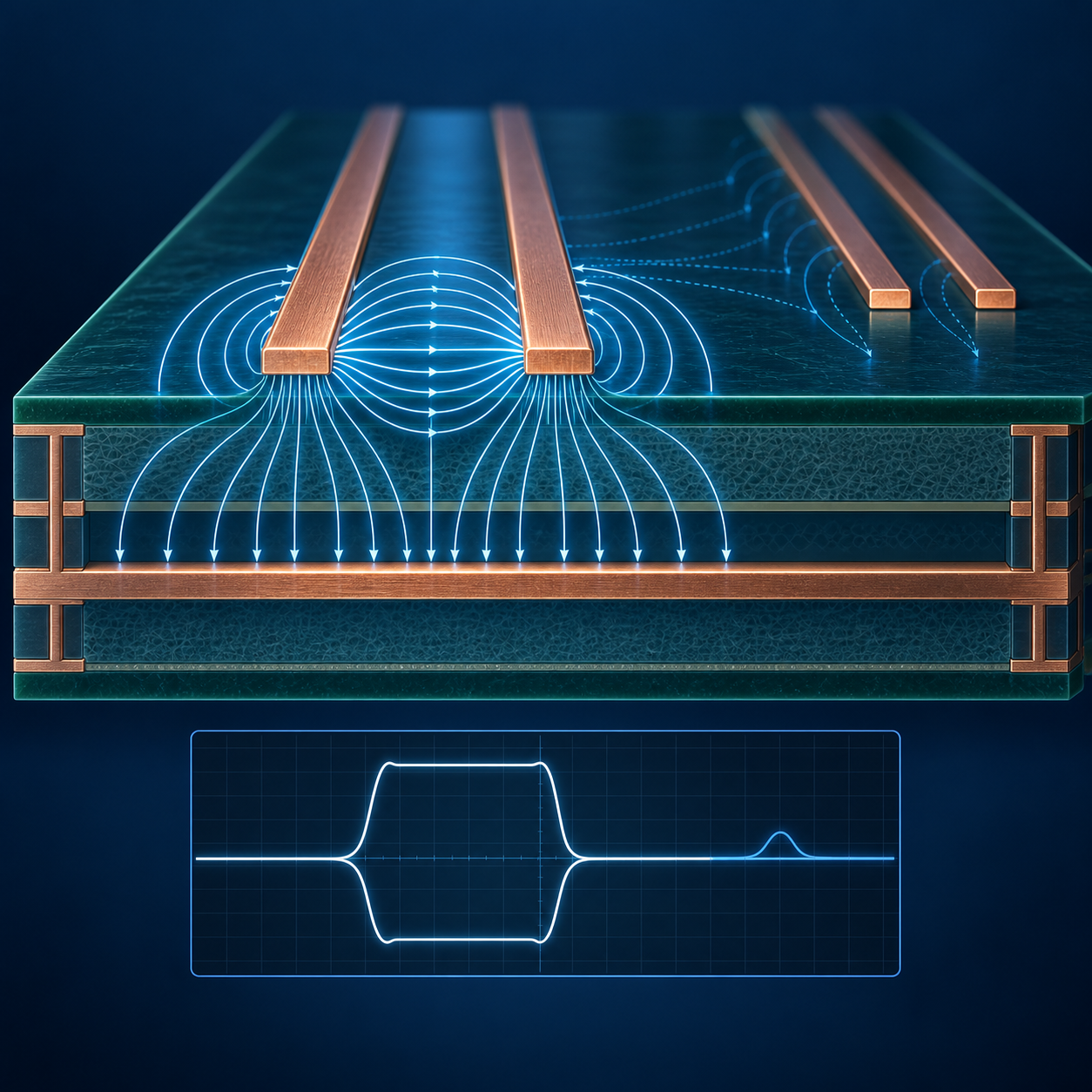
Differential Pair Impedance
Design a controlled-impedance differential pair: odd, even, differential and common-mode impedance, coupled geometries, routing, asymmetry and near-end crosstalk.
Written and technically reviewed byElectroDesignForge Engineering Team
View the editorial process📖 Definition
A differential pair consists of two traces carrying equal and opposite signals. Its behaviour is not defined by two independent single-ended impedances: electromagnetic coupling between the traces creates odd and even modes. Differential impedance, common-mode impedance, stack-up, symmetry, and return paths therefore have to be treated as one transmission-line problem.
What to specify
A requirement such as “100 Ω pair” is incomplete without context. It normally means differential impedance measured between the two conductors, but the result depends on geometry and return plane. A useful fabrication note ties the target to a specific layer and stack-up.
Layer: L3, stripline pair referenced to L2 and L4
Target impedance: 100 Ω differential
Tolerance: per the interface rule and fabricator capability
Geometry: finished width, edge-to-edge spacing and copper to be confirmed
Control: impedance coupon, compensated width and measurement report
Common 85 Ω, 90 Ω, and 100 Ω targets are not interchangeable. They depend on the interface, receiver, termination, and documentation for the exact part. Always use the target, tolerance, skew limits, and routing rules stated by the relevant component vendor or standard.
The Differential Pair & XTALK Calculator compares six coupled geometries, estimates modal impedances, and explores how spacing changes near-end crosstalk. It is a pre-layout tool: the final geometry remains the one validated by the PCB fabricator.
The four impedances to distinguish
A coupled pair is usefully described by two elementary excitations:
| Quantity | Excitation on both conductors | What it describes |
|---|---|---|
Odd-mode Zodd | Equal amplitude, opposite polarity | The intended differential operation |
Even-mode Zeven | Equal amplitude, same polarity | Common-mode behaviour |
Differential Zdiff | Voltage measured from P to N | The target normally quoted by an interface |
Common-mode Zcm | Both lines together with respect to the reference | Disturbance, balance, and common return behaviour |
For a symmetric pair using a common port convention:
Zdiff = 2 × Zodd
Zcm   = Zeven / 2
Those equations highlight an important point: a 100 Ω differential pair is not necessarily two 50 Ω single-ended lines. In the ideal symmetric case it corresponds to Zodd = 50 Ω, the impedance of either trace while the other is driven with opposite polarity. As traces move closer, coupling rises, Zodd falls, and Zdiff generally falls.
An asymmetric pair — with unequal width, return path, via, or nearby metal — converts some differential signal into common mode. Its average Zdiff may look acceptable while it still creates emissions, reduced margin, or compliance problems.
Intended coupling versus unwanted crosstalk
Within a pair, P-to-N coupling is intended: it helps establish differential impedance and concentrates fields. Crosstalk becomes a problem when another signal — the aggressor — interferes with a nearby pair or trace — the victim.
Two mechanisms coexist:
- Capacitive coupling injects current when aggressor voltage changes quickly.
- Inductive coupling is associated with aggressor current and magnetic field.
Their combination produces, among other effects, NEXT (near-end crosstalk): a pulse observed near the end where the transition was launched. The calculator reports a terminated NEXT estimate; use it to compare arrangements, not to guarantee complete-link margin. FEXT, reflections, vias, connectors, loss, and real terminations need a more complete simulation or measurement.
Compare the actual coupled length with rise time, not only clock frequency. A fast edge across a long parallel section can accumulate more disturbance than a high-rate signal with a slower edge. A sound practical rule is to enter the transmitter’s minimum rise time and the length over which the conductors really run side by side.
Pair geometries: edge-coupled or broadside-coupled
| Geometry | Construction | Strengths | Watch-outs |
|---|---|---|---|
| Edge-coupled microstrip | Two outer-layer traces side by side above one plane | Simple routing and inspection | Field partly in air and solder mask; more radiation and neighbour sensitivity |
| Edge-coupled embedded microstrip | Traces near one plane, under a dielectric layer | A compromise between surface access and confinement | Both dielectric distances and solder mask affect the result |
| Edge-coupled symmetric stripline | Inner traces between equally spaced planes | Strong confinement and good immunity | Pressed heights and finished copper are essential |
| Edge-coupled asymmetric stripline | Inner traces closer to one plane | Fits many practical stack-ups | Fields and returns become unbalanced if H1 and H2 are not defined correctly |
| Shielded broadside pair | Traces vertically aligned on adjacent layers between planes | Strong coupling in dense routing | Layer transitions and fabrication are more demanding |
| Unshielded broadside pair | Vertically aligned traces without nearby planes | Very strong direct coupling | Common mode and surrounding enclosure are highly influential; use only in a controlled case |
In every case, width W, edge-to-edge spacing S, copper thickness T, plane distances, and design Dk matter. One broad trend is useful for sanity checking: bringing the two traces closer increases coupling and often lowers Zdiff; moving the reference plane farther away raises impedance and weakens confinement. Those trends never replace a geometry-appropriate model.
Read the stack-up before choosing width and spacing
“FR-4, 1.6 mm, 1 oz” is not enough. For a controlled pair, request from the fabricator:
- Signal layers and continuous reference planes on either side.
- Pressed copper-to-plane distances — not only nominal prepreg thickness before lamination.
- Finished copper thickness, including outer-layer plating.
- Design Dk at the relevant frequency or stated method, together with its tolerance.
- Solder-mask presence, thickness, and Dk on outer layers.
- Etch constraints: finished width, minimum spacing, and proposed compensation.
Only freeze width and spacing after obtaining that stack-up. If the fabricator proposes a compensated width to meet impedance, preserve it in the fabrication data and do not change it locally without re-evaluating the pair.
A sizing workflow
- Obtain the interface target, tolerance, minimum rise time, length limits, and routing constraints.
- Choose a layer with a continuous reference plane and a geometry supported by the stack-up.
- Enter actual
W,S,T, Dk, and plane distances in the calculator. - Adjust width and spacing to reach the
Zdifftarget without violating fabrication rules or making routing fragile. - Review the separation between
ZoddandZeven, the coupling coefficient, and estimated NEXT for real neighbours and actual parallel length. - Obtain fabricator confirmation of the stack-up and compensation and, for a critical link, a coupon and measurement report.
Do not choose spacing from a slogan such as “three trace widths” or “three dielectric heights.” Those ratios cannot simultaneously account for Dk, planes, width, copper, nearby traces, and interface requirements. They are at most a placement starting point, never proof of impedance or crosstalk.
Routing: preserve electrical symmetry
Useful matching is electrical, not merely geometrical. Two traces of identical length can propagate differently if their environment changes. Keep both members together, on the same layer, and at constant separation wherever practical.
- Route P and N in parallel with identical width, spacing, and copper surroundings.
- Avoid placing a plane pour, board edge, dense ground-via field, or another trace close to only one member.
- Maintain a continuous return plane. Do not cross a slot, keep-out, or reference transition without a return path.
- At a layer change, use the same via structure for P and N and add return vias close to the transition when the reference plane changes.
- Minimise via stubs; backdrill or select a suitable via architecture when the signal budget requires it.
- Avoid sharp corners, neck-downs, and asymmetric pads. Curves or 45° segments do not substitute for discontinuity analysis.
Length-tuning meanders deserve special care. They bring a trace closer to itself and to its partner, adding local capacitance, coupling, and sometimes common mode. Add the minimum needed length using adequately spaced segments, and only apply length matching after checking the skew tolerance actually allowed by the protocol.
Connectors, components, and package escape
The trace section is only one link in the chain. Connector launches, BGA pads, cable or flex pairs, ESD devices, common-mode chokes, and vias can introduce a larger discontinuity than a few millimetres of well-sized trace. Check the component vendor’s reference layout: antipads, pad geometry, ground fencing, via count, backdrill, layer sequence, and any required termination.
A common-mode choke is not transparent by default. Select it using differential and common-mode parameters, imbalance, usable band, and S-parameter model when margin is tight. Place and route it symmetrically.
Fast-calculation limits
The Differential Pair & XTALK Calculator uses a quasi-static model. It is valuable for exploring geometric effects, synthesising spacing, and ranking risks, but it does not replace a 2D/3D field solver or production validation.
Use a more complete analysis when margin is tight, edges are very fast, the data rate is high, or the following effects matter: copper roughness, trapezoidal etch profile, glass weave, dispersion, loss, solder mask, vias, antipads, connectors, transitions, neighbouring pairs, FEXT, reflections, and non-ideal terminations. In every case, interface requirements and fabricator rules take precedence over a generic calculator result.
Pre-fabrication checklist
- Is the target explicitly differential, with verified tolerance and interface rule?
- Does the fabricator stack-up define pressed heights, finished copper, and Dk?
- Do P and N maintain symmetric geometry and surroundings, including at vias and pads?
- Is the return plane continuous along the route and through transitions?
- Have neighbours, parallel length, and rise time been assessed for crosstalk?
- Have connector launches, stubs, antipads, protection, and series components been reviewed?
- Does the fabrication note request the required compensation, coupon, and measurement report?
Bibliography
- IPC-2141A — Design Guide for High-Speed Controlled Impedance Circuit Boards.
- IPC-2221 — Generic Standard on Printed Board Design.
- H. A. Wheeler — foundational work on coupled lines and modal impedances.
- Interface documentation and layout guides from the relevant component or connector vendor.