
Microstrip and stripline impedance
Microstrip and stripline differences, stack-up parameters, the effect of width, dielectric and copper, and a method for specifying controlled impedance.
Written and technically reviewed byElectroDesignForge Engineering Team
View the editorial process📖 Definition
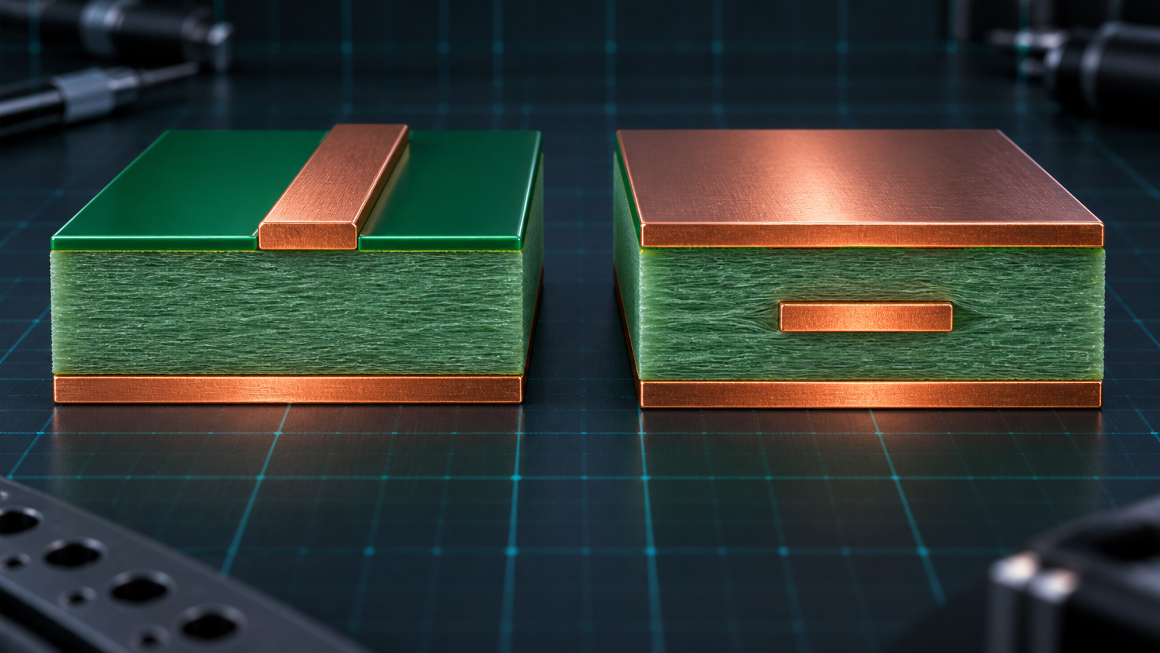
A microstrip is an outer-layer trace referenced to a plane on a nearby layer. A stripline is an inner-layer trace between two reference planes. In both cases, characteristic impedance depends on the complete electromagnetic geometry: trace width and thickness, distance to the planes, dielectric permittivity, solder mask and fabrication details.
Microstrip or stripline: choosing the geometry
| Geometry | Construction | Strengths | Watch-outs |
|---|---|---|---|
| Microstrip | Outer-layer trace above one plane | Easy access, often lower dielectric loss, straightforward routing and inspection | Field is partly in air and solder mask; more sensitive to nearby structures and radiation |
| Symmetric stripline | Inner-layer trace centred between two planes | Better field confinement, good immunity and low radiation | Higher dielectric loss; width may be narrower and depends on the pressed stack-up |
| Asymmetric stripline | Inner-layer trace closer to one plane | Fits a practical non-symmetric stack-up | Both dielectric heights must be known and maintained |
Microstrip is common for accessible surface signals, RF routing and interfaces where outer-layer routing is convenient. Stripline is often preferred for fast signals crossing a dense board or where emission and susceptibility need to be limited. This choice does not replace the need to manage vias, reference changes and fabrication constraints.
Use the PCB impedance calculator to compare these geometries using the fabricator’s actual stack-up.
What sets the impedance
For a single-ended line, the following variables have the strongest effect:
| Parameter | General effect when the parameter increases |
|---|---|
Trace width W | Impedance decreases |
Distance to the reference plane H | Impedance increases |
Relative permittivity εr / Dk | Impedance decreases |
Copper thickness T | Impedance decreases slightly, especially for narrow traces |
| Solder mask on a microstrip | Impedance usually decreases |
These trends help spot an inconsistency, but they are not enough to freeze a trace width. Microstrip equations use an effective permittivity εeff: part of the field travels in the dielectric and part in air or solder mask. Stripline is more fully confined in dielectric, so its effective permittivity is closer to the material Dk.
Reading a stack-up as an electrical specification
An indication such as “FR-4, 1.6 mm, 1 oz” is not enough to calculate impedance. You need the detailed stack-up at the signal layer:
- The signal layer and the continuous reference plane or planes surrounding it.
- The pressed distance between trace and each plane, not only the prepreg’s nominal pre-lamination thickness.
- The finished copper, including outer-layer plating where applicable.
- The material’s design Dk at the target frequency, supplied by the laminate or PCB manufacturer.
- Solder-mask presence, thickness and Dk for a microstrip.
- Finished-width, dielectric-height, copper and Dk tolerances.
For a microstrip, height H is the distance from trace to its return plane. In a symmetric stripline, the two plane distances are equal. An asymmetric stripline needs separate lower H1 and upper H2 heights; do not replace them with an average unless the model supports it.
A 50 Ω design example
Consider an outer microstrip above a ground plane. If etching makes the trace narrower, its capacitance per unit length falls and its impedance rises. If the pressed dielectric becomes thicker, coupling to the plane also falls and impedance rises. These two variations can therefore add together.
For a 50 Ω target, use the calculated width as a starting point, then ask the fabricator to confirm its impedance coupon and compensated width. A useful specification states at least:
Layer: L1 microstrip referenced to L2
Target impedance: 50 Ω single-ended
Tolerance: ±10%
Stack-up reference: fabricator stack-up revision X
Control: impedance coupon and measurement report
The Gerber width can be adjusted by the fabricator when it controls the stack-up and guarantees the target. Do not change that width after validation without repeating the analysis.
Return current and transitions
Impedance is not determined by the signal trace alone. At high frequency, return current preferentially follows the reference plane below a line, where coupling is strongest. A plane split, reference change, or layer transition without a return via creates a discontinuity that can degrade a signal even when every trace segment is 50 Ω.
- Keep a continuous reference plane under a microstrip and on both sides of a stripline.
- Place ground vias near layer transitions to provide a short return path.
- Do not force return current across a slot, keep-out or split plane.
- Check connectors, launches, vias and stubs: they often matter more than a few millimetres of correctly dimensioned line.
Fast-calculation limits
The PCB impedance calculator provides a single-ended quasi-static estimate and a tolerance envelope for comparing options. It does not replace a field solver or fabricator validation when margin is tight or data rate is high.
A more complete analysis is needed when solder mask, copper roughness, trapezoidal etching, glass weave, coupled differential lines, vias, connector launches, nearby planes, loss or frequency dispersion matter. For a standard interface, always start from its official impedance target and routing rules.
Pre-fabrication checklist
- Choose the geometry actually available in the stack-up: microstrip or stripline.
- Associate every line with a continuous return plane.
- Use the fabricator’s pressed dielectric and finished-copper data.
- State the target impedance, tolerance, layers, and single-ended or differential mode in the fabrication notes.
- Request compensated width, test coupon and measurement report when impedance is critical.
- Check transitions, vias and reference changes separately.
Bibliography
- IPC-2141A — Design Guide for High-Speed Controlled Impedance Circuit Boards.
- E. O. Hammerstad and Ø. Jensen — Accurate Models for Microstrip Computer-Aided Design, IEEE MTT-S, 1980.
- IPC-6012 — qualification and performance requirements for rigid printed boards, supplemented by fabricator rules and coupons.