
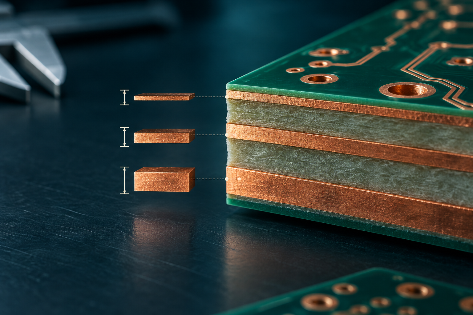
PCB copper thickness and copper weight
oz/ft² ↔ µm equivalence, common copper values, the distinction between base and finished copper, and consequences for routing and thermal design.
Written and technically reviewed byElectroDesignForge Engineering Team
View the editorial process📖 Definition
PCB copper is commonly specified either as an area weight in ounces per square foot (oz/ft²) or as a nominal thickness in micrometres (µm). They describe the same starting foil approximately: 1 oz/ft² is about 35 µm of copper.
Quick reference
| Copper weight | Nominal thickness | Common use |
|---|---|---|
| 0.25 oz/ft² | ≈ 9 µm | Fine-pitch inner layers, HDI stack-ups |
| 0.5 oz/ft² | ≈ 18 µm | Dense signal layers |
| 1 oz/ft² | ≈ 35 µm | General-purpose boards |
| 2 oz/ft² | ≈ 70 µm | Higher-current power paths |
| 3 oz/ft² | ≈ 105 µm | Power distribution, thermal spreading |
| 4 oz/ft² | ≈ 140 µm | High-current and industrial boards |
Use the oz ↔ µm converter to calculate intermediate values.
Why an ounce becomes a thickness
The “ounce” in a PCB stack-up is not a thickness unit. It is the mass of copper spread uniformly over one square foot of area. The resulting thickness depends on copper density and is conventionally rounded by the PCB industry:
thickness (µm) ≈ copper weight (oz/ft²) × 35
The inverse relation is:
copper weight (oz/ft²) ≈ thickness (µm) ÷ 35
This is a nominal conversion for design communication. IPC-4562B specifies copper foil by area weight and calculated thickness; use the fabricator’s material data when a tolerance is critical.
Base copper is not always finished copper
On an inner layer, the specified foil is usually close to the final conductor thickness after etching. On an outer layer, PCB fabrication adds copper during plated-through-hole and pattern plating. The finished trace can therefore be thicker than the starting foil.
| Drawing term | What it means | Design action |
|---|---|---|
| Base copper | Foil on the laminate before outer-layer plating | State it in the stack-up |
| Finished copper | Copper remaining on the finished outer trace after plating | Ask the fabricator for the target and tolerance |
| Copper in a via | Electrodeposited wall thickness | Specify separately from trace copper |
For example, “1 oz outer copper” can be ambiguous unless the drawing says whether it means base foil or finished copper. Put this distinction in the fabrication notes and agree it with the board house before release.
What changes when copper gets thicker
More copper reduces the resistance of a trace with the same geometry:
R = ρ × L / (w × t)
Where t is the copper thickness. Doubling t roughly halves the DC resistance, voltage drop and resistive dissipation, provided width, length and temperature stay comparable.
However, heavier copper also changes manufacturing constraints:
- Narrower gaps and traces become harder to etch consistently.
- More etch compensation may be needed, particularly on external layers.
- Controlled-impedance geometries change because conductor thickness is part of the field geometry.
- Thick copper helps spread heat, but it does not replace a complete thermal analysis.
Use the PCB track-width calculator for a first current and temperature-rise estimate, then verify clearances, finished copper and fabrication capability with the supplier.
Practical specification checklist
Before sending Gerbers or ODB++ data, record the following for every copper layer:
- Base or finished copper requirement.
- Nominal value in either oz/ft² or µm, plus the other unit where it avoids ambiguity.
- Layer function: signal, plane, high-current, RF or thermal spreader.
- Minimum trace/space, annular ring and copper-to-board-edge rules compatible with that copper weight.
- Required finished-hole plating and any impedance tolerance.
For current-carrying conductors, copper weight is only one variable. IPC-2152 also considers trace geometry, temperature rise, board construction, nearby planes, airflow and duty cycle.
Bibliography
- IPC-4562B — Metal Foil for Printed Board Applications, including copper foil area weights and calculated thickness.
- IPC-2152 — Standard for Determining Current Carrying Capacity in Printed Board Design.
- IPC-2221C — Generic Standard on Printed Board Design.