
PCB crosstalk: XTALK, NEXT, and FEXT
Understand PCB crosstalk: capacitive and inductive coupling, NEXT/FEXT, rise time, parallel length, spacing, noise reduction, and validation.
Written and technically reviewed byElectroDesignForge Engineering Team
View the editorial process📖 Definition
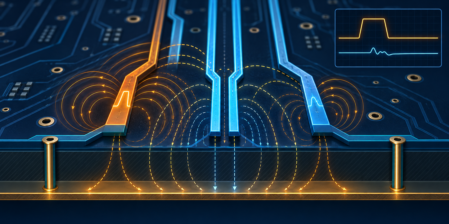
Crosstalk (XTALK) is unwanted disturbance transferred from an aggressor trace to a victim trace. It comes from the electric and magnetic fields shared by nearby conductors. On a fast PCB, it can reduce noise margin, shift a threshold, add jitter, or close an eye diagram even though the nets have no galvanic connection.
The problem: fields, not touching wires
Two nearby traces form both a small capacitance and inductively coupled loops. Every aggressor transition therefore injects a disturbance into the victim through both mechanisms:
| Mechanism | Origin | What raises crosstalk | Effect at the victim |
|---|---|---|---|
| Capacitive coupling | Electric field between conductors | Small gap, long parallel run, fast voltage edge | Current is injected while aggressor voltage changes |
| Inductive coupling | Magnetic field around the aggressor loop | Large return loop, close parallel traces, fast current change | Voltage is induced in the victim loop |
Both contributions occur at once. Depending on line structure and observation point, they can add or partly cancel. A trace over a continuous reference plane has a compact return loop: its field is more confined to that plane and less available to neighbours. Conversely, a trace far from its plane, a return forced around a plane split, or a long parallel run encourage coupling.
Crosstalk follows edge rate, not bit rate alone. A 10 MHz GPIO with a 500 ps rise time may be more aggressive than a higher-data-rate link with multi-nanosecond edges. Use the shortest realistic 10–90% rise time from an IBIS model, datasheet, or measurement.
Terms: aggressor, victim, NEXT, and FEXT
The aggressor is the switching net; the victim is the observed net. The disturbance can be measured at the near or far end of the parallel region:
| Term | Name | Where it is observed | Key point |
|---|---|---|---|
| NEXT | Near-End Crosstalk | At the victim end close to the aggressor source | The disturbance returns toward the near end; peak level depends on coupling and grows with parallel length until saturation |
| FEXT | Far-End Crosstalk | At the opposite victim end | It depends strongly on capacitive/inductive balance, structure, loss, and length |
NEXT is often the most direct metric for comparing two spacing choices in a routing corridor. FEXT still matters: in a homogeneous near-TEM structure, the two contributions can largely cancel; in microstrip, asymmetric geometry, or a real channel, they need not.
Reflections add another layer. A small disturbance at its origin can return from an unmatched termination, via, connector, or stub and land at a harmful point in the receive window. A single NEXT value is not, by itself, a channel-compliance verdict.
Parallel length and rise time: when the peak saturates
For its terminated coupled-line NEXT estimate, the Differential Pair & XTALK Calculator uses this pre-design relationship:
NEXT ≈ Va × Kb,term × min(1, 2 × td / tr)
td = Lcoupled × tprop
Lsat = tr / (2 × tprop)
| Symbol | Meaning |
|---|---|
Va | Aggressor step amplitude |
Kb,term | Coupling coefficient in the terminated model |
td | Propagation delay along the parallel region |
tr | Aggressor 10–90% rise time |
Lsat | Saturation length; above it, this NEXT peak estimate no longer rises |
For example, with 6 ps/mm propagation, a 300 ps edge, and 25 mm of parallel traces, td is about 150 ps. 2 × td / tr = 1, so peak NEXT has saturated in this model. Reducing the parallel run below 25 mm, increasing the gap, or slowing the edge reduces the estimate. Extending the region still changes coupling duration and possible reflections, but not this simplified peak.
The calculator helps compare options. It does not produce a complete waveform, solve FEXT, or model an unmatched coupled line. Use parameter extraction, a field solver, and channel simulation when margin is tight.
The PCB parameters that actually matter
| Parameter | Why it affects crosstalk | Practical action |
|---|---|---|
| Aggressor-to-victim spacing | A larger gap closes less field on the neighbouring conductor | Reserve clearance at placement, not only during routing |
Plane height H | A smaller H confines more field to the plane and reduces lateral spread | Route fast nets near a continuous reference plane when the stack-up allows |
| Co-parallel length | Exchanged energy grows with the close region until the edge reaches saturation | Separate routes early and avoid long shared corridors |
| Rise time | A short edge contains more high-frequency energy | Choose driver strength, series resistance, or slew-rate control when the interface permits it |
| Line structure | Microstrip, stripline, adjacent layers, and neighbouring copper expose fields differently | Use the real fabricated stack-up, not a generic nominal geometry |
| Return-current path | A discontinuity enlarges the loop and makes fields less predictable | Avoid plane splits; provide a nearby return at layer transitions |
Generic 3W, 3H, or 5H rules can guide first placement but are not universal guarantees. The right distance depends on the layer, edges, parallel length, victim sensitivity, and interface requirements. High-speed component guides often supply more applicable rules, especially between TX, RX, clocks, and other pairs.
Differential pairs: reduce external coupling, do not assume it disappears
A symmetric differential pair can reject a disturbance that reaches both conductors nearly equally; it does not make crosstalk disappear. A nearby trace, a parallel pair, an asymmetric via, or a reference change can couple differently into each conductor and convert part of the noise into a differential component visible to the receiver.
For crosstalk, distinguish two clearances:
- Within a differential pair, spacing is chosen to satisfy the interface’s impedance requirement. Do not change it as a quick external-coupling fix.
- Between pairs, or between a pair and another net, spacing limits unwanted coupling. Protect this gap during placement, especially in BGA, connector, and breakout areas.
Symmetric routing, continuous return current, and equivalent transitions remain important because they preserve common-mode rejection. They do not substitute for real aggressor-to-victim spacing.
Reducing crosstalk: priority order
- Separate aggressor and victim. Keep sensitive nets away from clocks, fast outputs, power-switching nodes, TX/RX pairs, and noisy connectors.
- Reduce parallel runs. Make routes diverge early; a brief crossing, preferably on orthogonal layers with continuous reference planes, is often better than a long side-by-side run.
- Bring signal close to its plane. A signal layer adjacent to a solid ground plane confines fields and gives predictable return current.
- Preserve returns. Do not cross a plane split. At layer transitions, place nearby ground-return vias when the return path needs them.
- Control edges. If protocol and timing budget allow, series resistance or slew-rate control can reduce high-frequency content and coupling.
- Isolate adjacent layers. Avoid long, co-parallel fast traces on adjacent signal layers. Prefer orthogonal directions when stack-up and return current allow it.
A copper guard or ground trace is not an automatic cure. Without suitable stitching vias it can become a floating conductor; with them it also changes impedance and routing space. Use it only when interface rules and stack-up analysis support it.
Symptoms and diagnostic method
Crosstalk is often intermittent: it appears when an aggressor switches as the victim nears a threshold. Look for the following:
| Symptom | Crosstalk clue | Useful check |
|---|---|---|
| Errors correlate with a clock or nearby channel | Failure follows activity on a specific net | Capture aggressor and victim together; temporarily change aggressor activity |
| Jitter or eye closure | Disturbance lands in the sampling window | Inspect an eye diagram or overlay acquisitions triggered from the aggressor |
| Repeating spur on an ADC or sensitive measurement | Noise tracks digital transitions | Compare spectrum or samples with and without neighbouring digital activity |
| Failure limited to one PCB revision or breakout area | Local geometry dominates | Inspect parallel lengths, anti-pads, layer changes, and reference planes |
Measure with a probe that has a very short ground connection, or use a differential probe where appropriate: a long ground lead can pick up field itself and imitate the effect you are trying to measure. TDR helps locate discontinuities; a VNA or channel extraction/simulation can quantify coupling in a critical geometry.
Common mistakes
| Mistake | Why it fails | Better approach |
|---|---|---|
| Checking bit rate only | Severity follows edge rate and repetition, not data rate alone | Use the shortest realistic rise time |
| Measuring gap without stating the convention | Rules and calculators can use edge-to-edge or centre-to-centre spacing | State the convention and retain the fabricator’s convention |
| Spacing traces only at a crossing | The long parallel section is still the region that accumulates coupling | Reduce the whole co-parallel length |
| Adding a guard trace without analysis | It may shift impedance or lack a proper reference | Check stack-up, stitching vias, and interface rules |
| Forgetting an adjacent layer | Two adjacent signal layers can couple strongly | Inspect routes and orientation across all layers |
| Concluding from one NEXT number | FEXT, reflections, loss, and sampling instant still matter | Validate the channel and critical timing case |
When a quick calculation is enough — and when it is not
The Differential Pair & XTALK Calculator suits exploration: compare a gap, layer, parallel length, and rise time before locking placement. It supplies a terminated NEXT estimate and highlights the edge saturation length.
Move to a field solver, RLCG extraction, and channel simulation when the signal is fast, noise margin is small, vias/launches/connectors dominate, or FEXT, loss, roughness, glass weave, and reflections can affect the result. Final validation can combine an impedance coupon, TDR, VNA, simulation, and eye measurement on representative hardware.
Anti-crosstalk checklist before release
- Fast aggressors and sensitive victims are identified in placement and routing.
- Long co-parallel regions are eliminated or supported by analysis.
- Clearances derive from stack-up, edge rate, and noise margin—not from one generic rule alone.
- Every fast trace has a continuous reference plane and a short return path through transitions.
- Adjacent signal layers do not carry long, co-parallel fast routes.
- Driver edges are checked in the shortest realistic rise-time case.
- Critical channels receive analysis or measurement appropriate to their margin.
Bibliography
- Intel — Agilex 7 Device Family High-Speed Serial Interface Signal Integrity Design Guidelines, PCB-trace section.
- Intel — AN 224: High-Speed Board Layout Guidelines, crosstalk section.
- Analog Devices — AN-1177: LVDS and M-LVDS Circuit Implementation Guide.
- Analog Devices — AN-1364: Differential Filter Design for a Receive Chain in Communication Systems.
- Howard Johnson and Martin Graham — High-Speed Digital Design: A Handbook of Black Magic.