SPI interface: modes, timing and wiring
Understand CPOL, CPHA, MOSI, MISO, SCLK and CS, then build a reliable SPI bus with timing, logic levels, topologies and debugging guidance.
Written and technically reviewed byElectroDesignForge Engineering Team
View the editorial processReference guide
SPI (Serial Peripheral Interface) connects a controller to nearby ICs such as Flash memories, ADCs/DACs, displays, sensors and RF devices. This synchronous serial link is fast and full duplex, but it is not a complete standard: framing and electrical limits come from each datasheet.
Quick reference
| Signal | Direction from controller | Function | Key point |
|---|---|---|---|
| SCLK / SCK | output | Serial clock | Its idle level is set by CPOL. |
| MOSI | controller → peripheral | Data transmitted | Also called COPI, SDI or DIN. |
| MISO | peripheral → controller | Data received | Also called CIPO, SDO or DOUT; high impedance when unselected. |
| CS / SS / nCS | output, often active-low | Selection and frame boundary | One independent CS is normally needed per peripheral. |
| GND | shared | Reference and return path | Keep it alongside signals, especially off-board. |
MOSI and MISO assume the controller viewpoint. COPI (Controller Out, Peripheral In) and CIPO (Controller In, Peripheral Out) make the roles clear when discussing a link without a schematic.
SPI defines neither addressing, acknowledgement nor a universal maximum rate. The application protocol defines commands, register addresses, dummy bytes and responses. A logic analyser can therefore decode valid bits while a device stays silent because CS or command framing is wrong.
Check before wiring: logic levels, allowed SCLK rate, SPI mode, MSB/LSB order, word length, CS active state and CS timing. 1.8 V, 2.5 V, 3.3 V and 5 V domains are not automatically compatible.
The four modes: CPOL and CPHA
- CPOL (clock polarity) sets idle SCLK: 0 = low, 1 = high.
- CPHA (clock phase) sets the sampling edge. With CPHA = 0, the first edge after CS samples the first bit; with CPHA = 1, it changes that bit and the following edge samples it.
| Mode | CPOL | CPHA | SCLK idle | Sample edge | Data changes on |
|---|---|---|---|---|---|
| 0 | 0 | 0 | Low | Rising | Falling |
| 1 | 0 | 1 | Low | Falling | Rising |
| 2 | 1 | 0 | High | Falling | Rising |
| 3 | 1 | 1 | High | Rising | Falling |
The leading edge is the first transition away from idle and the trailing edge is the second. CPHA = 0 samples on the leading edge; CPHA = 1 samples on the trailing edge. This works for either CPOL setting.
Reading a timing diagram
- Check SCLK before CS: that is CPOL.
- Find the edge where stable data is read: that is CPHA.
- With CPHA = 0, the first bit must be valid before the first edge.
- Confirm output delays in the datasheet; data does not always change exactly on the opposite edge.
Wrong CPHA often shifts bits; wrong CPOL reads a plausible sequence at the wrong instants. 0x00, 0xFF or an invalid ID are possible symptoms, not conclusive diagnoses.
Timing beyond frequency
| Parameter | Meaning | Risk when violated |
|---|---|---|
fSCLK | maximum clock rate | Intermittent errors or unstable sampling |
tSU(D) | MOSI/MISO setup before sample edge | Bit read at the wrong level |
tH(D) | Data hold after sample edge | Next bit corrupts current bit |
tCSS | active CS to first SCLK edge | First command ignored or shifted |
tCSH | last edge to inactive CS | Last bit not accepted |
tCSHI | CS inactive time between frames | Internal state not reset |
tDO | MISO output delay | Sampling too early at high speed |
The timing budget includes level-translator delay, trace or cable flight time, real edge rate and capacitive load. A rate that works on a short board can fail after adding a connector or branch.
For the usual active-low CS: keep SCLK at its CPOL state, assert CS, wait tCSS, present the first bit early enough for CPHA = 0, generate edges, then wait tCSH before releasing CS. Some parts require CS low across an entire command-address-data sequence; others execute an operation when CS rises.
Wiring MOSI, MISO, SCLK and CS
Controller MOSI  ─────────►  Peripheral SDI / DIN
Controller MISO  ◄─────────  Peripheral SDO / DOUT
Controller SCLK  ─────────►  Peripheral SCK
Controller nCS   ─────────►  Peripheral nCS
GND              ─────────►  GND
MISO may only be shared when every unselected peripheral really becomes high impedance. A pull resistor sets an idle state but never resolves two active outputs fighting each other.
SCLK is often most critical: it switches every bit, synchronises every receiver and can ring. Keep it short, over a continuous ground plane and away from sensitive analogue inputs. A series resistor of a few tens of ohms at the driver may damp a point-to-point connection; validate the value with an oscilloscope.
CS permits only one peripheral to answer. A pull-up toward inactive is useful during controller reset, after checking internal pulls, power consumption and rise-time needs.
SPI topologies
Star with independent CS
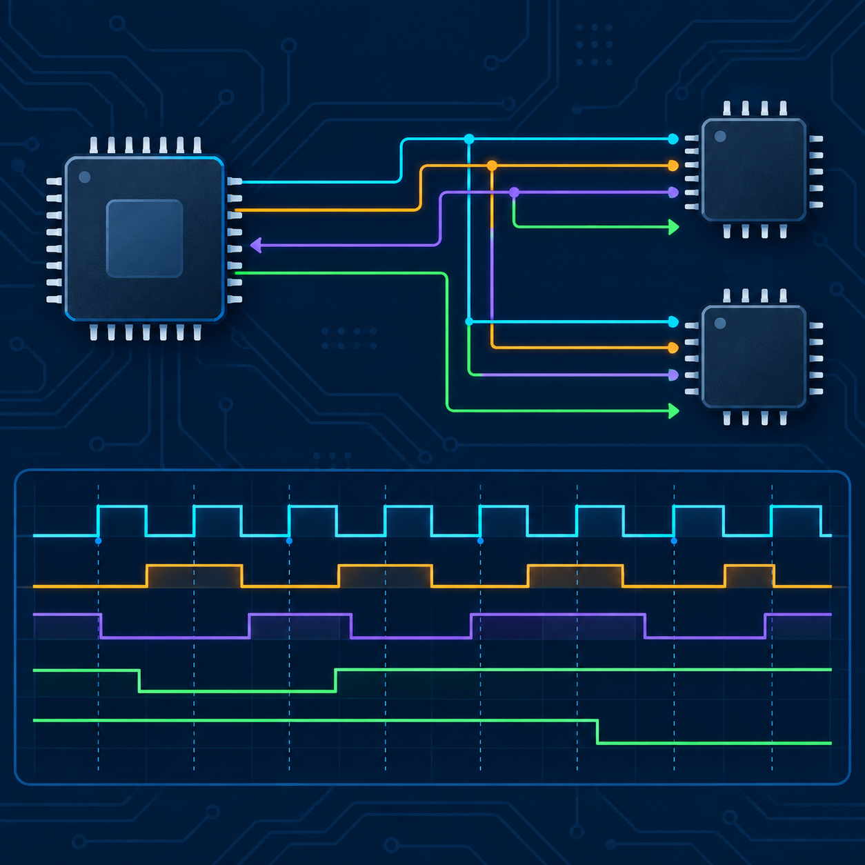
SCLK and MOSI go to every IC; every IC receives its own CS. Only the selected part drives MISO.
                  ┌──────────► Peripheral A
Controller ─ SCLK ├──────────► Peripheral B
           ─ MOSI ├──────────► Peripheral C
           ─ MISO ◄────────── shared outputs, high impedance when unselected
           ─ CSA  ───────────► A
           ─ CSB  ───────────► B
           ─ CSC  ───────────► C
This is the recommended topology: it is straightforward to debug and does not route bytes through other devices. When GPIOs are scarce, a decoder or expander can generate CS signals; include its delay and power-up state in the design.
Daisy chain
Some shift registers and LED drivers are designed for daisy chains. Their serial output feeds the next input; they share SCLK and CS.
Controller MOSI ─► Device 1 ─► Device 2 ─► Device 3
Controller SCLK ─► all devices
Controller CS   ─► all devices
Controller MISO ◄─ final device output, if available
Frame length is the sum of all device words and physical order determines byte order. This is not appropriate for normal SPI peripherals that simply share a bus.
Shared bus and signal integrity
Each branch is a stub that degrades edges as SCLK increases. Prefer compact distribution and short branches. For cable or board-to-board links, reduce fSCLK, provide a close ground return and measure at the receiver. SPI is not a differential interface designed for long distances.
| Situation | Recommended practice |
|---|---|
| One IC, very short traces | Direct connection; validate mode and logic levels |
| Several ICs on one board | Independent CS, MISO high impedance when unselected |
| SCLK ringing | Series resistor near controller; inspect with oscilloscope |
| Cable or interconnect | Lower rate, interleave GND, limit length, use transceiver if needed |
| Many CS lines | Decoder, shift register or expander with safe power-up state |
Logic levels and debugging
Compare VIH/VIL thresholds and absolute maximum ratings in both directions. A 1.8 V MISO can be too low for a 3.3 V input; a 5 V output can damage a non-tolerant 3.3 V input. Bidirectional MOSFET translators common in I²C are not automatically suitable for fast SCLK or MOSI: choose a buffer or translator rated for the chosen levels, rate and load.
- Start with one peripheral at 100 kHz or below.
- Check power, GND, reset and CS state before data.
- Measure SCLK, CS, MOSI and MISO together, triggered by active CS.
- Verify CPOL/CPHA, bit order and exact edge count per frame.
- Read a documented ID or status register, then raise the rate gradually.
A logic analyser checks protocol; an oscilloscope is required for edges, overshoot, noise and reflections. Probe near the peripheral input: measuring only at the controller can hide a line problem.
Checklist
- CPOL, CPHA, bit order and word length explicitly documented in schematic and firmware.
- One CS per peripheral unless a datasheet-defined chain is used.
- MISO released when unselected; no output contention.
- Logic thresholds, absolute maximums and timing checked in both directions.
- Short SCLK over continuous ground; any series resistor validated.
- Safe CS state during reset and power-up.
- Receiver-side measurement after adding cable, connector, translator or branch.
References
- NXP — SPI Block Guide, rev. 3.0
- Microchip — SPI Serial Interface
- Selected controller and peripheral datasheets: their modes, timing, levels and frame sequences take precedence over these general conventions.