
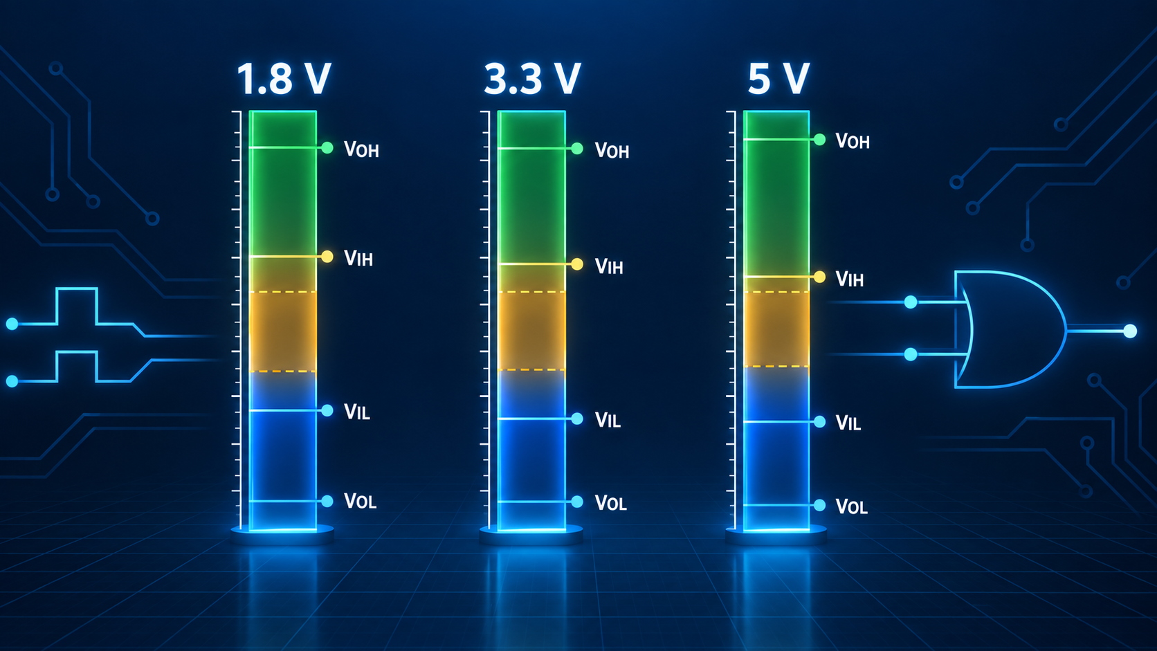
TTL and CMOS logic levels
Understand VIL, VIH, VOL, and VOH, verify noise margins, and design safe interfaces between 1.8 V, 3.3 V, and 5 V domains.
Written and technically reviewed byElectroDesignForge Engineering Team
View the editorial processKey point: an output is compatible with an input only when its worst-case guaranteed levels meet that input’s thresholds across supply, temperature, and load current. A nominal 1.8 V, 3.3 V, or 5 V label alone is not enough.
Quick reference
| Symbol | Meaning | Check |
|---|---|---|
| VIL | highest input voltage guaranteed LOW | VOL,max ≤ VIL,max |
| VIH | lowest input voltage guaranteed HIGH | VOH,min ≥ VIH,min |
| VOL | highest LOW output voltage | specified at a sink current |
| VOH | lowest HIGH output voltage | specified at a source current |
The region between VIL,max and VIH,min is undefined for a digital input. It is not a usable control level.
1. Inputs and outputs: keep the four specifications separate
I means input and O means output. Input limits say what a receiver accepts; output limits say what a driver guarantees.
| State | Input guarantee | Output guarantee |
|---|---|---|
| LOW | VIN ≤ VIL,max | VOUT ≤ VOL,max at IOL |
| HIGH | VIN ≥ VIH,min | VOUT ≥ VOH,min at IOH |
Use guaranteed min/max limits, not typical plots, to design an interface. VOH may be close to VDD with no load, yet fall materially when the output sources current.
Static noise margins
NMH = VOH(min, driver) − VIH(min, receiver)
NML = VIL(max, receiver) − VOL(max, driver)
Both margins must be positive. Larger margins tolerate more noise, ground shift, cable drop, and part variation. They do not replace checking rise time, capacitive loading, and absolute maximum ratings.
2. CMOS thresholds: often supply-relative
Many conventional CMOS families specify input thresholds near:
VIL(max) ≈ 0.3 × VDD
VIH(min) ≈ 0.7 × VDD
This is a useful rule of thumb, not a universal requirement. Modern CMOS may use fixed thresholds, TTL-compatible inputs, Schmitt triggers, or dedicated I/O standards.
| CMOS domain | Indicative VIL,max | Indicative VIH,min | Undefined region |
|---|---|---|---|
| 1.8 V | 0.54 V | 1.26 V | 0.54 to 1.26 V |
| 3.3 V | 0.99 V | 2.31 V | 0.99 to 2.31 V |
| 5.0 V | 1.50 V | 3.50 V | 1.50 to 3.50 V |
A 3.3 V CMOS output therefore cannot normally guarantee the HIGH required by a 5 V, 0.7 × VDD CMOS input. Conversely, a 5 V output can exceed a 3.3 V input’s electrical limit even when its logic level is easy to read.
3. TTL: why 3.3 V can work, but is not a universal rule
Historic 5 V bipolar TTL typically uses fixed input limits: VIL,max = 0.8 V and VIH,min = 2.0 V. A 74LS HIGH output may only be guaranteed to 2.7 V under its stated light load, while a LOW output can be guaranteed up to about 0.4 or 0.5 V at the stated current.
| Representative 5 V TTL interface | LOW | HIGH | Consequence |
|---|---|---|---|
| Input | VIL,max = 0.8 V | VIH,min = 2.0 V | a 3.3 V HIGH is usually recognised |
| 74LS output, light load | VOL,max ≈ 0.4 V | VOH,min ≈ 2.7 V | may not meet a 5 V, 30/70% CMOS input |
Many modern “TTL-compatible” or LVTTL devices retain the 2.0 V HIGH threshold while operating from 3.3 V. TTL in an I/O table then describes the thresholds, not necessarily the internal technology or 5 V tolerance.
4. 1.8 V, 3.3 V, and 5 V compatibility
The following assumes a push-pull output and an ordinary input. Treat it as a starting point; the two actual datasheets decide the design.
| Driver → receiver | Threshold reading | Electrical limit | Practical verdict |
|---|---|---|---|
| 1.8 V CMOS → 3.3 V CMOS | 1.8 V is below typical 3.3 V VIH | no overvoltage | No without translation |
| 3.3 V CMOS → 1.8 V CMOS | HIGH may be logically sufficient | 3.3 V often exceeds 1.8 V VIN,max | Unsafe without a tolerant input or translator |
| 3.3 V CMOS → 5 V TTL | 3.3 V > 2.0 V | check receiver input limit | often logic-compatible; verify power domain |
| 5 V TTL → 3.3 V CMOS | HIGH is readable | 5 V can damage the 3.3 V input | No without adaptation or 5 V tolerance |
| 5 V TTL → 5 V CMOS | matching voltage domain | check current and speed | normally intended use |
| 5 V CMOS → 5 V TTL | VOH comfortably exceeds 2.0 V | check input current | normally compatible |
Two independent checks
- Logic compatibility: compare VOH,min with VIH,min, and VOL,max with VIL,max.
- Electrical compatibility: check VIN,max, absolute maximum ratings, pin currents, and the condition when the receiver is unpowered.
An input labelled “5 V tolerant” addresses only part of the electrical question. It does not by itself guarantee threshold compatibility, power-off injection behaviour, or tolerance in every pin mode.
5. Worked example: 3.3 V GPIO to a 5 V TTL input
Suppose a GPIO guarantees VOH,min = 2.9 V at the selected load and VOL,max = 0.4 V. The TTL input requires VIH,min = 2.0 V and accepts VIL,max = 0.8 V.
NMH = 2.9 V − 2.0 V = 0.9 V
NML = 0.8 V − 0.4 V = 0.4 V
Both margins are positive, so the logic levels are compatible. Still check that the TTL pin has no pull-up to 5 V and no input-current condition that back-powers the GPIO while it is off. A 3.3 V GPIO is not automatically safe with a resistor pulled to 5 V.
6. Pull-ups, open drain, and the pull resistor
An open-drain output actively drives only LOW. A pull-up resistor creates HIGH, so its rail determines both the HIGH level and the overvoltage risk.
For pull-up RP to VPU with total leakage Ileak, a first HIGH bound is:
VHIGH ≈ VPU − Ileak × RP
RP(max) ≤ (VPU − VIH(min)) / Ileak
The LOW bound comes from current when the line is pulled down:
RP(min) ≥ (VPU − VOL(max)) / IOL(max)
Then check RC rise time. Too large a resistor gives a slow edge; too small a resistor increases LOW-state current. Use the Pull-up / Pull-down Calculator to size the range from thresholds, GPIO current, capacitance, and rise-time target.
Do not improvise these cases
- A 5 V pull-up on a 3.3 V pin is permitted only when that exact pin and mode are explicitly 5 V tolerant, including when unpowered.
- Push-pull outputs must not be tied together. Wired logic needs compatible open outputs.
- A Schmitt input helps with slow edges but does not make an overvoltage safe.
- Bidirectional MOSFET translators suit some open-drain buses, not push-pull high-speed signals without timing analysis.
7. Schematic and prototype verification method
- Identify every exact pin type: input, push-pull, open drain, Schmitt, analogue, strap, or special-tolerance input.
- Extract guaranteed VIL, VIH, VOL, and VOH at the product’s supply, temperature, and current.
- Calculate NMH and NML; a negative margin requires translation or a different architecture.
- Check VIN,max, absolute maximum ratings, protection diodes, and partial-power-down behaviour.
- Include internal and external pull resistors in the current path. Parallel resistors and opposite rails can produce an intermediate level.
- Measure at the receiver with an appropriate probe: edge shape, overshoot, ground bounce, minimum VOH, and maximum VOL at real load.
Common pitfalls
| Mistake | Why it fails | Correction |
|---|---|---|
| Comparing only 3.3 V and 5 V | Threshold and electrical limits are separate. | Perform logic and electrical checks. |
| Using VDD as VOH | A loaded output may not reach its rail. | Use VOH,min at required current. |
| Treating typical as guaranteed | Temperature, process, and load vary. | Use datasheet min/max values. |
| Ignoring the unpowered domain | A protection diode can partially power a device. | Check partial-power-down and injection-current rules. |
| Adding a pull-up by intuition | It may use the wrong rail or be too strong. | Calculate resistor limits and rise time. |
Associated tool
Open the Pull-up / Pull-down Calculator to find a resistor range consistent with logic thresholds, GPIO current, line capacitance, and rise time.
Sources
- Texas Instruments — Logic Guide and 74xx/LVC/AHC family datasheets.
- Nexperia — application notes and CMOS / TTL-compatible logic family datasheets.
- The two actual component datasheets: DC electrical-characteristics tables, absolute maximum ratings, and power-sequencing requirements.