I²C bus: wiring, addressing, and pull-up resistors
Wire a reliable I²C bus: SDA and SCL roles, 7-bit addresses, speeds, bus capacitance, rise time, and pull-up sizing.
Written and technically reviewed byElectroDesignForge Engineering Team
View the editorial processKey point: I²C connects multiple ICs through two shared lines:
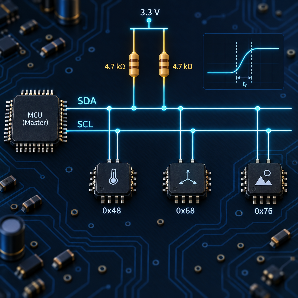
SDAfor data andSCLfor clocking. The outputs are normally open-drain: a device pulls a line LOW, while pull-up resistors return it HIGH. Sizing must satisfy both the LOW-level sink-current limit and the rise-time limit set by speed and total bus capacitance.
Quick reference
| Mode | Maximum SCL frequency | Maximum t_r rise time (30–70%) | Reference capacitance per line |
|---|---|---|---|
| Standard-mode (Sm) | 100 kHz | 1000 ns | 400 pF |
| Fast-mode (Fm) | 400 kHz | 300 ns | 400 pF |
| Fast-mode Plus (Fm+) | 1 MHz | 120 ns | 550 pF |
These limits come from the I²C specification. The slowest part may require a lower speed. Do not select Fm+ simply because a controller supports it: every target, level shifter, and isolator must support it too.
SDA and SCL: shared lines
SDA carries the address, read/write bit, data bytes, and acknowledges. SCL times the transfer. At idle, both lines are HIGH. A START is SDA falling while SCL is HIGH; a STOP is SDA rising while SCL is HIGH.
During data transfer, SDA stays stable while SCL is HIGH. The controller sends eight bits, then releases SDA on the ninth clock; the receiver pulls SDA LOW for an ACK or leaves it HIGH for a NACK.
                 +3.3 V                         +3.3 V
                   |                              |
                  [Rp]                           [Rp]
                   |                              |
SDA  ──────────────+──── controller ── target A ── target B
SCL  ──────────────+──── controller ── target A ── target B
GND  ───────────────────── common to every device
Use one effective pull-up on SDA and one on SCL. Multiple modules may already include them, making them parallel. Two 4.7 kΩ resistors make 2.35 kΩ; four make 1.18 kΩ. Check module schematics before adding another pair.
Why open-drain?
A device never actively drives the bus HIGH: it releases a line or pulls it LOW. If two devices act together, LOW wins without a short circuit between opposing output stages. This wired-AND behaviour enables acknowledge, multi-controller arbitration, and clock stretching.
SCL can sometimes be push-pull in a single-controller system with no clock-stretching targets; document that exception explicitly. For a portable compatible I²C bus, keep SCL open-drain with its pull-up.
Wiring, ground, and voltage levels
Connect all devices in parallel: SDA to SDA, SCL to SCL, and shared ground. Avoid a star with long branches; stubs add capacitance, reflections, and noise sensitivity. On a PCB, keep signals short, over a continuous ground plane, and away from fast switching nodes.
The pull-up rail sets the HIGH level. It must be compatible with every I/O, including an unpowered microcontroller. Do not directly connect a 1.8 V part to 3.3 V pull-ups unless its datasheet allows it. Use an I²C-suitable level shifter, with pull-ups on both sides when its circuit requires them.
Microcontroller internal pull-ups are often 20 to 100 kΩ: sometimes acceptable at very low speed on a short trace, but normally too weak for loaded 100/400 kHz buses. Check the actual value.
Addressing: 7-bit, not 8-bit
Most ICs use a 7-bit target address. The first byte on the wire is:
[ A6 A5 A4 A3 A2 A1 A0 | R/W ]
The R/W bit is added on the bus; it is not part of the 7-bit library address. A target at 0x68 appears as 0xD0 for write and 0xD1 for read. An API asking for 0xD0 may follow an 8-bit convention—check it before shifting an address twice.
ADDR, SA0, or SDO pins on many sensors select an address. Tie them to a defined level and record addresses in the schematic. If fixed-address targets collide, use an I²C multiplexer, another controller, or a different part variant. Ten-bit addressing exists but is uncommon; an internal sensor register is not the I²C address.
Speed, SCL, and clock stretching
SCL frequency is a maximum timing rate, not guaranteed payload rate: addresses, registers, ACK/NACK bits, START/STOP conditions, and internal delays reduce throughput. A 400 kHz multi-register transfer therefore takes longer than its byte count divided by 400 kbit/s.
A target can hold SCL LOW after the controller releases it: this is clock stretching. The controller must sample SCL and wait for HIGH, within the product timeout policy. Verify compatibility because some drivers handle it poorly. In multi-controller use, the device that releases SDA but reads LOW loses arbitration and stops.
Bus capacitance and rise time
Each line is an RC load: IC inputs, traces, cables, probes, connectors, and stray capacitance add up. When no device pulls a line LOW, the pull-up charges that capacitance gradually.
For a 30% to 70% VDD measurement:
t_r ≈ 0.8473 × R_p × C_bus
R_p,max ≈ t_r,max / (0.8473 × C_bus)
Use ohms, farads, and seconds. This gives the maximum pull-up resistance; above it, the rise is too slow. At 400 kHz with C_bus = 100 pF:
R_p,max ≈ 300 ns / (0.8473 × 100 pF) ≈ 3.54 kΩ
4.7 kΩ draws little current, but is too large to meet 300 ns with 100 pF. 3.3 kΩ is a better starting point, subject to LOW-current limits and measurement. Prefer measuring capacitance on the final assembly; otherwise add input capacitance, cable data (pF/m), connectors, and PCB margin. A probe adds capacitance too.
Pull-up sizing: a window, not a magic value
A smaller resistor speeds the edge but increases current while a device drives LOW. The lower limit is:
R_p,min ≈ (VDD − V_OL,max) / I_OL,max
For VDD = 3.3 V, V_OL,max = 0.4 V, and I_OL,max = 3 mA:
R_p,min ≈ (3.3 − 0.4) / 3 mA ≈ 967 Ω
R_p,min ≤ R_p ≤ R_p,max
The selected value is valid only in this window. If no window exists, reduce capacitance, lower speed, use a suitable I²C buffer, or use an Fm+-capable device with greater sink current. Do not choose below R_p,min just because it appears to work: V_OL can become ambiguous and dissipation rises.
| Situation | Starting point | Verify |
|---|---|---|
| Short PCB, 3.3 V, 100 kHz | 4.7 to 10 kΩ | capacitance and existing pull-ups |
| Short PCB, 3.3 V, 400 kHz | 2.2 to 4.7 kΩ | t_r and every target’s I_OL |
| Cable or many modules | calculated, often lower | sink current, EMC, waveform at cable end |
These ranges do not replace calculation for your assembly.
Measure and troubleshoot
Observe SDA and SCL at the endpoint farthest from the controller. Measure t_r from 30% to 70% of VDD, and check V_OL, ringing, and SDA stability while SCL is HIGH.
| Symptom | Likely causes | Actions |
|---|---|---|
| No targets found | missing ground, wrong address, swapped SDA/SCL | check continuity, power, 7-bit scan |
| Lines always HIGH | missing pull-up or wrong rail | check both resistors and their rail |
| Line stuck LOW | target in reset, wiring fault, interrupted transaction | isolate modules and reset the segment |
| Random NACKs | slow rise, noise, excess capacitance or speed | measure t_r, decrease R_p, slow bus |
| Fails only with all modules | parallel pull-ups too strong or cumulative capacitance | calculate equivalent resistance and capacitance |
A typical recovery releases SDA, generates up to nine SCL pulses, then a STOP. Use it only when all datasheets allow it; segment reset can be more robust.
Pre-layout checklist
- Do all parts share ground and compatible bus voltage?
- Do SDA and SCL each have one effective pull-up, without accidental parallel additions?
- Are addresses unique and listed in 7-bit form?
- Is the speed supported by every target, shifter, and isolator?
- Do
R_p,minandR_p,maxbound the selected value? - Is rise time verified on the board with real capacitance?
Associated calculator
- Open the Pull-up / Pull-down Calculator to calculate the resistance window from
VDD, GPIO current, thresholds, line capacitance, and I²C rise-time limit.
Sources
- NXP Semiconductors, UM10204 — I²C-bus specification and user manual: protocol, electrical levels, and Sm/Fm/Fm+ timing.
- Datasheets for the controller, targets, shifters, buffers, and isolators used: they take priority for
I_OL,V_OL, input capacitance, and clock-stretching support.