
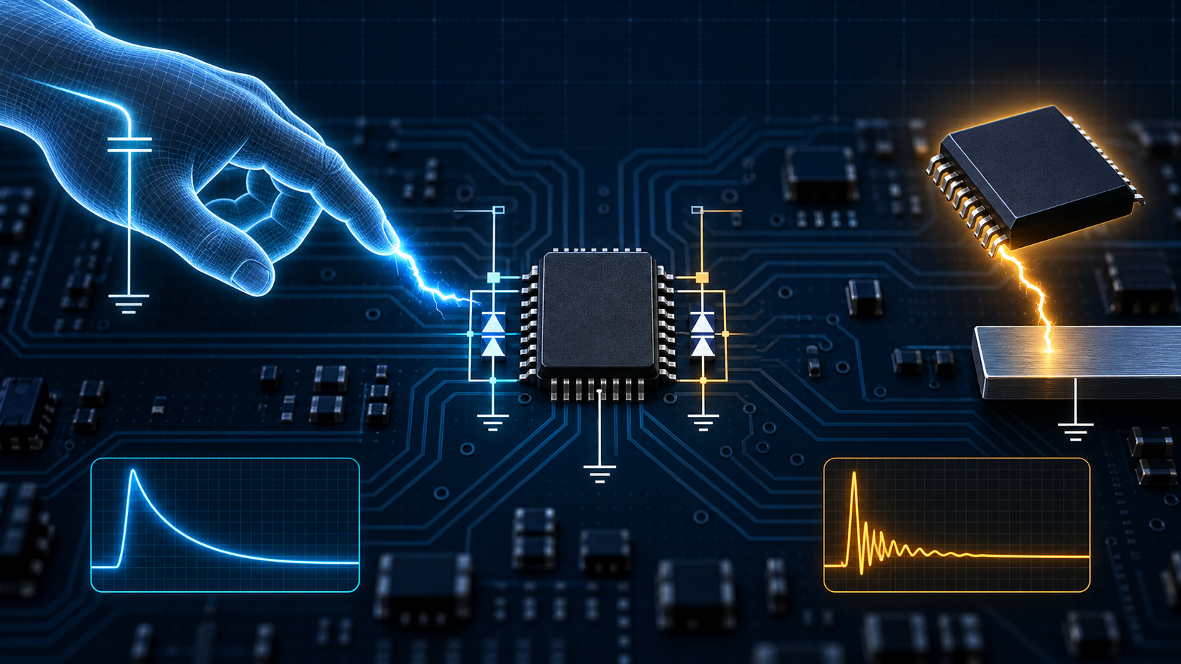
ESD levels and HBM/CDM models
Understand HBM and CDM ESD levels, waveforms, sensitivity classes, limits, and the consequences for component qualification and board design.
Written and technically reviewed byElectroDesignForge Engineering Team
View the editorial process📖 In brief
HBM (Human Body Model) and CDM (Charged Device Model) levels state a component’s withstand capability against two standardized, device-level electrostatic-discharge events. HBM represents a charged person touching a pin; CDM represents a charged component touching a conductive surface. Their voltages are not interchangeable, and neither result replaces IEC 61000-4-2 system-level testing.
Why ESD Damages Components
An electrostatic discharge transfers stored charge into a circuit extremely quickly. Even an event a person cannot feel can exceed the capability of a gate oxide, junction, fine metal trace, or input protection network because of its current and current slew rate.
Damage can be immediate — a short, open, or excessive leakage — or latent: the part still passes a functional test but has lost reliability margin. An HBM or CDM value in a datasheet is therefore a sensitivity classification for a defined test scenario, not a promise that a product will survive every discharge at the same voltage.
Keep these three ideas separate:
| Term | What it evaluates | Do not confuse it with |
|---|---|---|
| HBM / CDM | ESD robustness of a component or integrated circuit | Immunity of the assembled product |
| IEC 61000-4-2 | ESD immunity of accessible equipment or a system | HBM/CDM qualification of a chip |
| EOS | Electrical damage from overvoltage, overcurrent, or sustained energy | A standardized ESD pulse |
A passing HBM/CDM qualification never removes the need for board-level ESD design and relevant system testing.
The Two Events Being Modelled
| HBM — Human Body Model | CDM — Charged Device Model | |
|---|---|---|
| Physical situation | A charged person touches a pin or package. | The device is charged, then one pin touches a lower-potential conductor. |
| Main stored energy | A standardized 100 pF capacitor. | The capacitance of the device, package, and field plate. |
| Discharge path | 1.5 kΩ series resistance. | Very-low-impedance contact. |
| Signature | Damped pulse, typically on the order of 150 ns. | Much faster, package-dependent pulse, often under 2 ns. |
| Main risk | Energy and current injected into protection paths. | Very high current slew rate, ringing, and local current distribution in the package. |
| Current joint standard | ANSI/ESDA/JEDEC JS-001-2024. | ANSI/ESDA/JEDEC JS-002-2022. |
The tests are complementary. A component can have a good HBM rating and still be CDM-sensitive, especially in a small package with a low-inductance return path or during automated handling.
HBM: A Charged Person Discharging
An HBM generator charges a 100 pF capacitor and discharges it into the device under test through a 1.5 kΩ series resistor. It represents contact from the fingertip of a standing person to a conductive device connection.
A simplified circuit is:
high-voltage source → C = 100 pF → switch → R = 1.5 kΩ → DUT pin
As a first approximation, peak current is:
Ipeak ≈ VHBM / 1,500 Ω ≈ 0.67 A/kV
For example, a 2 kV stress has a nominal peak current near 1.33 A before fixture parasitics and the device response are included. The energy initially stored in the capacitor is:
E = ½ × C × V²
At 2 kV and 100 pF, that is 0.2 mJ. Energy alone does not describe the hazard: waveform shape, current path, and protection triggering are decisive.
The typical HBM leading edge is a few nanoseconds, followed by damped decay. The 1.5 kΩ resistance limits current, making HBM far less abrupt than CDM.
HBM Classification Levels
The classes below are recent ESDA/JEDEC HBM sensitivity classes. They are classification test conditions, not operating voltages.
| HBM class | Classification voltage range |
|---|---|
| 0Z | < 50 V |
| 0A | 50 V to < 125 V |
| 0B | 125 V to < 250 V |
| 1A | 250 V to < 500 V |
| 1B | 500 V to < 1,000 V |
| 1C | 1,000 V to < 2,000 V |
| 2 | 2,000 V to < 4,000 V |
| 3A | 4,000 V to < 8,000 V |
| 3B | ≥ 8,000 V |
A commonly quoted 1 kV HBM target is a design or qualification target; it is not permission to relax manufacturing ESD controls. Lower sensitivity or a different protection architecture may be justified by speed, leakage, capacitance, or supply-voltage constraints.
CDM: The Device Is the Charge Source
In a CDM event, a device acquires electrostatic charge — for example while moving through a feeder, tape, tray, or automated machine — and a pin suddenly contacts a conductor at a lower potential. The charge on the device itself is then released through that pin.
The standardized field-induced CDM method places the device on a field plate, charges it, then discharges each relevant pin at positive and negative polarity. Package geometry, size, metal content, lead height, and parasitic capacitance directly change the current waveform; there is therefore no universal CDM capacitor analogous to HBM’s 100 pF.
The contact has very low impedance. Current can reach tens of amperes for an extremely short time, and the entire event can be under 2 ns. That speed is why package inductance, return paths, and pin geometry matter as much as the ESD clamp itself.
CDM Classification Levels
| CDM class | Classification test condition |
|---|---|
| C0a | < 125 V |
| C0b | 125 V to < 250 V |
| C1 | 250 V to < 500 V |
| C2a | 500 V to < 750 V |
| C2b | 750 V to < 1,000 V |
| C3 | ≥ 1,000 V |
CDM voltage alone cannot determine current or energy delivered into the die. Two packages of the same silicon can produce different CDM behaviour. A useful test report therefore identifies the standard, revision, package, pin plan, and polarity instead of only saying “CDM 500 V.”
Why 1 kV HBM Does Not Equal 1 kV CDM
The volts are the models’ initial charge voltage, but the equivalent circuits differ. Comparing voltage alone is a common mistake.
| Question | HBM | CDM |
|---|---|---|
| Where is the capacitance? | In the generator, fixed at 100 pF. | In the device and fixture, so it depends on the package. |
| What limits current? | Mainly the 1.5 kΩ series resistor. | Mainly parasitic inductance and resistance in the contact path. |
| How fast is the stress? | A few-ns rise and decay on the order of hundreds of ns. | A sub-nanosecond edge is possible; event duration is around ns. |
| What must protection address first? | ESD conduction paths and clamp energy capability. | Very fast current distribution in the package and locally exposed inputs. |
A clamp robust enough for HBM energy can be too slow or too remote to limit a local CDM overshoot. Conversely, increasing HBM protection aggressively may add capacitance or leakage and degrade an RF, high-speed, or precision port. The ESD target is therefore a process, package, and system trade-off that should be verified with both methods where applicable.
Reading a Datasheet Correctly
A line such as HBM ±2 kV, CDM ±500 V should be read methodically:
- Identify the standard and revision: JS-001, JS-002, AEC-Q100, and an internal method are not automatically equivalent.
- Check whether the level is a target, guaranteed minimum, highest passing level, or a typical value.
- Confirm the tested package. CDM is especially dependent on it.
- Read the polarity, pins, and failure criteria. Not every pin is necessarily equivalent.
- For automotive use, check additional AEC-Q100-002 (HBM) and AEC-Q100-011 (CDM) requirements, including sequence and number of discharges.
- Do not apply the result to a user-accessible interface until system immunity, external diodes, grounding, and cabling have been validated.
When a supplier lists only an ESD voltage without the standard, package, or polarity, request the associated qualification report or compliance statement.
Board-Design Consequences
HBM and CDM qualify the chip; a board exposed through cables, connectors, buttons, or metal enclosure parts must also steer energy into an external, controlled path.
Accessible Interfaces
- Place the TVS or protection network as close as possible to the connector to minimize current-loop area and inductance.
- Give the protection a short, wide, low-inductance return to the appropriate chassis or reference plane.
- Do not route the transient through sensitive areas, flexes, noisy grounds, or the IC’s internal diodes.
- Select a TVS using operating voltage, clamp voltage, pulse current, parasitic capacitance, and the intended system standard; “ESD rated” without conditions is insufficient.
High-Speed, RF, and Analogue Ports
Protection capacitance and non-linearity can degrade signal integrity, noise, or calibration. Check bandwidth, S-parameters, or capacitance at the actual bias point, and optimize routing plus the ground return. An external protector cannot repair a long return loop.
Manufacturing and Handling
HBM/CDM results help size an ESD-control programme: EPA, grounding, wrist and footwear systems, ionization where an insulator cannot be grounded, dissipative or shielding packaging, feeder control, and training. ANSI/ESD S20.20 is intended for this kind of programme for ESD-sensitive items.
Common Errors
| Error | Why it is risky | Better practice |
|---|---|---|
| “8 kV HBM means IEC 61000-4-2 compliant” | The models, current, network, and test level differ. | Qualify the product to IEC 61000-4-2 when its interface is accessible. |
| “The TVS automatically protects the IC” | Placement and return path can still permit a local overshoot. | Minimize the connector–TVS–reference loop. |
| “HBM level is enough” | A chip can be much more CDM-sensitive. | Read and specify both HBM and CDM. |
| “Higher is always better” | Robustness can trade against leakage, capacitance, area, and performance. | Define a justified target and ESD-control strategy. |
| “An antistatic bag is enough” | Some bags dissipate charge without shielding a field or external discharge. | Use packaging appropriate to sensitivity and transport risk. |
ESD Specification Checklist
- Separate internal components from interfaces actually accessible to a user.
- Ask the supplier for HBM and CDM levels with standard, revision, package, polarity, and pass definition.
- Set device-level HBM/CDM requirements from the manufacturing flow, package, and application.
- Set system-immunity requirements, such as IEC 61000-4-2, separately for external interfaces.
- Size the external network at real current: trigger voltage, clamp voltage, capacitance, and mounting inductance all matter.
- Simulate or measure the return path and inspect placement before adding a larger protector.
- Establish ESD controls for assembly, test, storage, and transport.
- Validate the finished product with the contractual methods and levels, not only the IC’s ESD datasheet entry.
References and Standards
- ANSI/ESDA/JEDEC JS-001-2024 — Human Body Model (HBM), device level
- IEC 60749-28:2022 / ANSI/ESDA/JEDEC JS-002 — Charged Device Model (CDM), device level
- EOS/ESD Association — Fundamentals of ESD, Part 5: Device sensitivity and testing
- EOS/ESD Association — HBM and CDM classification levels
- ANSI/ESD S20.20 — Electrostatic-discharge control programme
- IEC 61000-4-2 — Electrostatic-discharge immunity at system level